To this point in the chapter, we have presented a brief introduction to semiconductors and have described the interface that develops when they are put into contact with an electrolyte. Current flow under dark conditions has also been described. Finally, we looked briefly at the light absorption characteristics of semiconductors. We are now ready to combine light and electrochemistry to explore photoelectrochemistry.
The absorption of light discussed in the previous section results in the excitation of an electron to the conduction band and the formation of an electron–hole pair. We would like to use the energetic electrons that are created to perform work by driving nonspontaneous electrochemical reactions. In order to do so, we need a way to separate the electrons and holes. Otherwise, the electron–hole pairs formed by light absorption will be lost to recombination. In a traditional solid-state solar cell, that separation is done by the electric field that exists at the junction between n-type and p-type materials. The electric field causes the electrons to move in one direction and the holes to move the other direction, effecting the desired separation.
As discussed above, an electric field is also present at a semiconductor–electrolyte interface. This field can be used to separate the electron–hole pairs, as illustrated in Figure 15.19a. To be separated, the electron–hole pairs must be generated in the space-charge layer (depletion region) where the field exists, or sufficiently close to that zone so that the charge carriers can diffuse to the zone before they are recombined (more on this shortly). The physical situation is illustrated in Figure 15.19b. The electron–hole pairs that are generated are separated by the field in the depletion zone. The strength of the electric field is enormous, and allows for effective collection of minority carriers at the surface of the semiconductor before they can undergo recombination. For an n-type semiconductor, the photogenerated minority-carrier holes migrate to the semiconductor–electrolyte surface, and the electrons migrate away from the surface to the bulk of the semiconductor and are collected at the back contact. The photoproduced current (n-type semiconductor) is anodic and associated with the movement of holes (the minority carrier) to the semiconductor–electrolyte interface. This anodic current is in contrast to the cathodic current produced by a forward bias in the dark. The photocurrent is often limited by the generation rate of electron–hole pairs and is thus directly connected to the rate of absorption of light in and near the depletion zone; “near” is interpreted as within a diffusion length, Lp, as defined below. The total current is simply the sum of the photocurrent and the potential-dependent majority current considered in a previous section. The relevant expression for an n-type semiconductor is
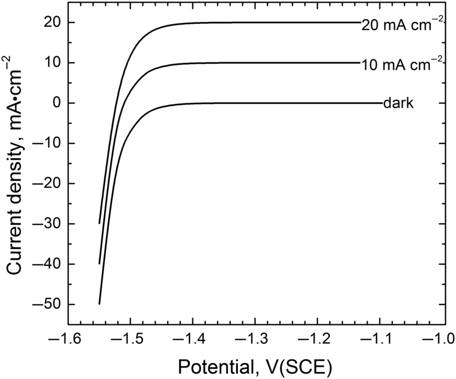
The photogenerated anodic current (iph), which results from the movement of photogenerated holes (minority carrier), is positive and dominates when the interface is reverse biased. In contrast, the current is dominated by the flow of electrons (majority carrier) under conditions of forward bias. The shape of the current–voltage curve is shown in Figure 15.20 where the magnitude of iph depends on the level of light absorption as indicated in the figure. An analogous expression can be written for a p-type semiconductor, although the photocurrent would be negative (cathodic), and the forward bias would be at positive potentials and correspond to anodic current.
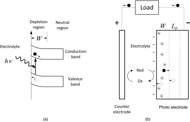
The Gärtner equation, written for an n-type semiconductor, provides a simplified expression for the photocurrent based on the absorption of light in the depletion region (0 ≤ x ≤ W) and within the diffusion region where holes are sufficiently close to the depletion zone to diffuse to the zone before recombining (see Figure 15.19).
where ![]() is positive as it enters the semiconductor and the distance W is measured from the surface where the light enters. Remember that iph is positive (anodic) for n-type semiconductors and negative (cathodic) for p-type semiconductors. Comparison of Equation 15.22 with Equation 15.18 shows that the additional diffusion term increases the light absorption for a given distance W into the semiconductor. The diffusion region is characterized by the diffusion length, Lp, defined as
is positive as it enters the semiconductor and the distance W is measured from the surface where the light enters. Remember that iph is positive (anodic) for n-type semiconductors and negative (cathodic) for p-type semiconductors. Comparison of Equation 15.22 with Equation 15.18 shows that the additional diffusion term increases the light absorption for a given distance W into the semiconductor. The diffusion region is characterized by the diffusion length, Lp, defined as
(15.23)![]()
where DP is the diffusivity of the minority carriers and τP is the recombination time for the holes. The quantum yield, defined mathematically as
(15.24)![]()
can be readily obtained from Equation 15.22, where ![]() is the entering light flux, as defined previously in conjunction with Equation 15.18. It turns out that for high-quality semiconductors such as silicon, the effective minority carrier diffusion length is much greater than the depletion region width, and the collection of photogenerated carriers is nearly independent of the applied potential and the depletion region width. For semiconductors with low lifetimes (small effective diffusion lengths), it is necessary to account for carrier collection that depends on the depletion region width and the potential.
is the entering light flux, as defined previously in conjunction with Equation 15.18. It turns out that for high-quality semiconductors such as silicon, the effective minority carrier diffusion length is much greater than the depletion region width, and the collection of photogenerated carriers is nearly independent of the applied potential and the depletion region width. For semiconductors with low lifetimes (small effective diffusion lengths), it is necessary to account for carrier collection that depends on the depletion region width and the potential.
Leave a Reply